
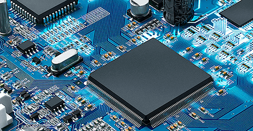
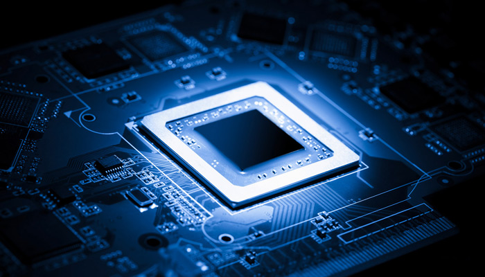
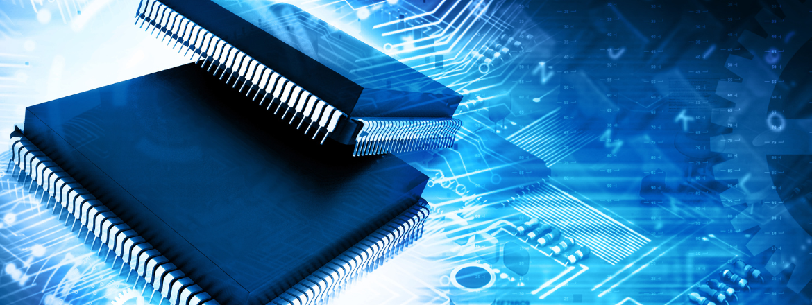
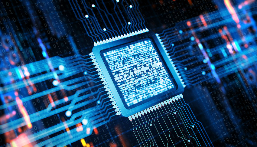
When you look at the integrated circuits, all you see is just a very small chip, but this small-sized chip is designed to hold all the electronic components that an electronic circuit would have.
This single chip contains the entire circuit board with all the essential active and passive components fabricated through a chip design process carrying out essential functions.
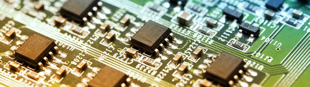
Integrated circuits are essential to the electronics industry; almost every appliance contains a printed circuit board, and IC is the main unit. Therefore, in every application around us, we can see the presence of integrated circuits.
If you are looking forward to knowing more about these integrated circuits, you are at the right place. In this guide below, we have highlighted the essential details you must know. So, let’s read the guide below:
Definition of Integrated Circuit
An integrated circuit design comprises a series of electronic circuits, which are on a base of semiconductor material; it is made of silicon in most cases. Integrated circuits are also referred to as ICs, ASICs, or just a chip.
This small chip contains many small MOSFETs (Metal Oxide Semiconductor Field Effect Transistors); these are placed over the flat board creating a circuit board design and connected to create an integrated circuit. These circuits are smaller, offer speedy performance, and are affordable compared to the discrete counterparts manufactured with the help of discrete electronic components.
The electronics industry relied on transistors before integrated circuit IC came into being, but because of the benefits offered by integrated circuits, it shifted to invest in these chips to have in their electronic devices.
Integrated circuits offer mass production and are reliable; compared to individual circuits, integrated circuits provide excellent performance at an affordable cost.
The main reason for the better performance of ICs is that they consume less power than the discrete circuits since their switch times are very short, and the low power consumption makes them suitable for every electronic device.
On the other hand, the cost is low because, using the photolithography process; the ICs are printed as one unit and are not constructed like a transistor. Hence, these IC packages need lesser material than the discrete components.
It is not just that ICs are only advantageous; in fact, there are disadvantages too, and that is the involvement of high cost in the fabrication process of their photolithography masks.
Hence, the ICs are expensive for smaller quantity production. In contrast, they are suitable for high-volume production so that they can offer higher profits when manufactured for multiple practical applications.

Brief History of Integrated Circuits
The semiconductor industry has a massive role in the integrated circuit design process. The metal oxide silicon-made semiconductor device fabrication and the related advancement in technology are what that has given birth to ICs.
ICs were floated in the market in the 1960s, and when compared to what they are today, a massive difference can be seen in terms of their dimensions and speed. Hence, with the latest innovations and technological advancement, more circuits now fit on this chip design with the same small size.
The concept of bonding several electronic components on one device started with the evolution of vacuum tubes in the 1920s, but their creation aimed to avoid tax. In Germany, the radio receivers were implied with taxes depending on the number of tube holders they had. Hence, to adjust the tubes in one holder, this approach of developing a vacuum tube was carried out.
The very first concept of IC packages took place in the year 1949 when Werner Jacobi, a German engineer, filed a patent. It was filed for an amplifying device that was an integrated circuit looking like a semiconductor device. It was used in hearing aids, which were smaller and cheaper.
Jack Kilby brought an idea in 1957 when he decided to create ceramic substrates in smaller or micro modules. He worked on creating a chip design that comprised all the components present in the electronic circuits to be fabricated on the semiconductor silicon material, and this started the integrated circuits.
However, the idea presented by Kilby in the form of integrated circuits was equipped with limitations, and the major one was the need for more possibility of mass production. It had many wires present externally that caused it to hinder the manufacturing of these circuits in ample quantity.
Hence, keeping this limitation in mind, Robert Noyce created a monolithic integrated circuit chip, which was more practical than Kilby’s design.
After this came Fred Heiman and Steven Hostein, who introduced the RCA; after that, General Microelectronics successfully designed the commercial MOS IC.
In today’s time, the manufacturing of significantly smaller sizes of transistors has become very difficult. Hence, most companies look forward to multiple techniques that help with the improved performance of this chip without leading to reduce the size of the transistors.
Therefore, many kinds of ICs based on multiple packages are floated, like multi-chip modules, ICs with three dimensions, etc. Such ICs provide for a high bandwidth memory, and that was too using the creation of silicon vias through the process of die stacking.
Importance of Integrated Circuits
Integrated circuits are commonly used in many electronic appliances, and this is because it contains many electronic components that create simple as well as complex circuits within this chip.
Due to the smaller size and high functionality of ICs, the different electronic gadgets can perform much faster and are even compact and lightweight. In the absence of these integrated circuits, the gadgets would have been much slower, huge, and heavy.
The integrated circuit board can perform as an operational amplifier, timer, counter, logic gates, microprocessor, and much more and is the primary building block in most modern electronic appliances and gadgets.
Despite having a small outline package, these chips comprise the capability to carry out multiple functions ranging from the ability to conduct electricity to act as analog to digital converters and digital to analog converters.

How are Integrated Circuits Made?
An integrated circuit will have many electronic components like capacitors, resistors, transistors, and diodes that are surface mount over a silicon base. The process of manufacturing integrated circuits is a very extensive one.
When the first IC was developed, it was eminent that silicon could be used to manufacture multiple electronic components, but the main idea was how to make and connect them through the same silicon piece.
Hence, by altering and doping the chemical composition of the silicon crystal’s tiny areas, the regions were produced that help improve the mounting style to create an integrated circuit.
The different regions created on the surface of the silicon base were bonded together, and, with the bonding of two regions, the third region was created called as depletion region.
The process helped create a P-N junction, which led to insulating or conducting electricity depending on the side over which voltage was applied since the chip had a positive and negative side.
At one time, hundreds of ICs are manufactured, and thin slices of silicon are cut to create these chips. The manufacturing process needs to be carried out in an environment that is clean and does not contain any air particles. In fact, during the process, the machinery operators in the room wear lint-free garments to avoid the dust particles being stuck to the silicon.
In many cases, some of the components of ICs are light sensitive; hence, the light sources must be filtered while manufacturing occurs.
Types of Integrated Circuits
Integrated circuits are not just one kind of chip; there are three kinds of integrated circuits, each of which has a distinct functionality. These are discussed below:
Digital Integrated Circuits
The digital integrated circuits aid the direction of data that flows. It also carries out the mathematical estimation process, which uses the binary digits zero and one. Digital circuits are widely used to support computer system function through their binary data flow.
The digital integrated circuit is meant to receive readings that have precise values. Digital integrated circuits do not operate over a consistent range of signal amplitudes; they operate over some of the defined levels only.
The main building block of digital circuits is the logic gates that work on two signals, 0 and 1. These digital circuits are widely used on computers, frequency range counters, modems, enterprise networks, etc.
Analog Integrated Circuits
The process of analog integrated circuits is to act as amplifiers, modify, and filter the signals. They are the simplest integrated circuits because of their minor components.
They perform the function of sending and receiving signals in multiple devices. An analog integrated circuit is used in devices that respond to continuous signal variations.
The analog integrated circuits are used in analog applications like op-amps, where they carry out the performance of the continuous variable output based on the signal level that is being input. There are many different examples of applications of analog integrated circuits like sensors, operational amplifiers, and power management circuits.
Mixed-Signal Integrated Circuits
Another kind of integrated circuit is known as mixed-signal ICs; these circuits in the underlying physics prove to be an IC, which is a special one. It contains the particular functions of analog design ICs and digital ICs. Such circuits are mostly used as radio frequency circuits.
They carry out functions like analog to digital converters and digital to analog converters and therefore are called mixed signal circuits. These chips are minor and have a very affordable cost, but they can consider signal interference. Hence it could be called as a mixture of analog and digital circuits.
Design and Fabrication of Integrated Circuits
The process of designing and fabricating the integrated circuits is very detailed, and before fabrication, the design process takes place. Below you will learn about the design and fabrication process involved in the integrated circuits.
Overview of the Design Process
The integrated circuit is, in most cases, an off-the-shelf item; it is standard, and once the design has been created, no further work is required. Such standard ICs would comprise most analog switches, voltage regulators, and converters for analog to digital and vice versa.
Such an integrated circuit IC is mainly sold to companies that use them to produce printed circuit boards that could further be used in electronic appliances.
Apart from these, there may be other integrated circuits that are used to have some extensive design requirements, for instance, microprocessors used for computers. Such a product will need a lot of research and, after that, achieves the final output.
The flow of IC design can be seen in two categories: analog integrated circuits and digital circuits.
In the case of digital circuits, the design will comprise manufacturing components that increase memory like RAM, ROM and flash, microprocessors, ASICs, etc., and this is looking forward to creating maximum circuit density by the circuit designers. To achieve this, circuits are placed in such a manner that timing signals, and clocks are provided with a proper route.
In the case of analog integrated circuits, the analog design offer specialization in the power IC design. It is used in op-amps and linear regulators in active filters. This design mainly concentrates on the underlying physics comprising resistance, power dissipation, and gain. Analog circuit board also needs a larger active area than digital integrated circuits.
The Integrated Circuit Fabrication Process
The fabrication process for integrated circuits is a detailed one and has many steps involved within it; some of these steps involved in the fabrication process are discussed below:
Preparation of Silicon Wafer
A cylindrical piece of silicon with a diameter between 1.5 inches to 4 inches is placed inside a heated vacuum chamber with a coil; the silicon piece is encircled with this coil. A high temperature is then created within the vacuum, which is heated to allow silicon to reach its melting point of around 1400C.
When the silicon keeps on melting, the impurities within it are transferred to the coil and it moves down from the cylinder of silicon carrying all the impurities with it. As these impurities reach the end of the cylinder, the bottom portion is sliced, leaving behind the pure silicon cylinder.
The cylinder is then taken out and using a wafer slicer, a thin round silicon wafer is then cut, and the surface over which these ICs are to be created is subjected to polishing.
To form an insulation base, the surface of the wafer is subjected to a layer of silicon dioxide, and it keeps the chip free of oxidation of silicone that might lead to cause impurities.
To achieve this piece of silicon cut from the cylinder is subjected to a very high heat steam that is around 1000C so that the pressure created by water vapor leads to allow silicon to react with it.
However, while this process is carried out, the temperature and the time for such steam exposure are controlled to control the silicon dioxide layer over the IC.
Masking
The process of designing complex circuits over an IC chip is more or less the same as the one carried out for the printed circuit board; the only difference is that ICs have relatively smaller dimensions, comprising multiple layers superimposed over each other.
Every layer is designed using a CAD machine, and after an image is created, it is masked and transferred to the wafer’s surface after being reduced. This mask is a mix of opaque and transparent in different areas and has the images of hundreds of ICs that are needed to be created on the wafer.
In the middle of the silicon, a photoresist material is placed and subjected to being spun, which helps to distribute the material all over the surface of the wafer. After the material is spread over the surface, the wafer is baked so that the solvent can be removed.
The wafer, which is now coated, is placed under the first mask layer, which is irradiated using light due to the lack of space between the circuits. Hence, ultraviolet light is introduced between the layers to irradiate the photoresist.
After this, the mask is removed, and the areas having photoresist are also dissolved; now, the negative photo-resisted areas are left, and the positive ones are dissolved. The uncovered areas are etched, and then the doping process takes place so that the layer of PN regions can be created.
Oxidation
The process of adding oxygen is known as oxidation; when it comes to integrated circuits, or you can call them semiconductor devices, these are made with silicon, and when they react with oxygen, silicon dioxide is formed.
This process of oxidation in fabricating integrated circuits requires it to be carried out in a furnace with a very high temperature, and it could be either dry oxidation or wet oxidation.
Steam is used in the wet oxidation process, and both processes will offer great electrical and insulation to the chip. Moreover, the covering of silicon dioxide protects the wafer to get any kind of impurities.
Doping – Atomic Diffusion
The dopants can be added by creating a layer of two regions, P and N, called atomic diffusion. In this technique, the batch of wafers is subjected to an oven and comprises a heating element, the wafers are subjected to a heating temperature of more than 800 C, and the dopant chemical is then subjected to the inert gas.
When the dopant and the inert gas pass over the wafers, the deposits of the dopant are left on the areas that remain unexposed to the masking process. This doping method is suitable for larger areas but will not go well with smaller portions; when carried out repeatedly, it can cause problems.
Doping – Ion Implantation
Another method to carry out the doping process is to add dopants through ion implantation. In this method, a gas for dopant, which may be either boron tri-chloride or phosphine, is ionized by allowing a beam of ions with high energy to be fired at regions of the wafers. The beam of ions allows these ions to penetrate and remain in the wafer by implanting.
The penetration’s depth can easily be controlled by changing the beam’s energy and the amount of dopant introduced. This process is somewhat like firing a beam in the cathode ray tube and doesn’t require any masking and rather directly points the dopants where they are needed.
Making successive layers
The entire process of doping and masking is repeated for all the layers, and this is how the circuit chips are completed. Sometimes silicon dioxide is used as a layer through chemical vapor deposition to have insulation between the layers.
In this process, the surface of the wafer is heated, and a reaction occurs between the oxygen and silicon that creates a silicon dioxide layer over the IC chip. It makes the contact pads and the final layer seal the surface. In this stage, the ICs are seen tested for their functionality.
MetaLlization
The metallization process comprises adding a metal layer on the surface of integrated circuits. The coating may be zinc, silver, or aluminum, and CMOS circuits are usually coated with aluminum. This will help protect the ICs from dust, water, and air to protect them from damage.
The components within the integrated circuits are even connected through metallization. the metal layer is first placed on the surface of the wafer, and then the interconnected area is etched. The metallization process applies this metal layer using a chamber, and the wafer is kept inside a chamber, allowing coating on the entire surface.
Making individual ICs
This wafer created is like a glass piece and consists of hundreds of IC chips that are separated through a process where using a diamond cutter, the ICs are separated, and then the wafer is subjected to pressure to separate individually.
If any ICs are failed in the electrical test, they are removed and discarded. The rest of these are checked for damages; if they are damaged in the separation process, they are discarded.
The ICs in good condition are bonded in the surface mount packages, and the wires are connected through either thermo-compression or ultrasonic bonding; the package is marked with the details.
Packaging the ICs
These ICS are even sealed in anti-static plastic bags and then ready to ship. The process of packaging also comprises assembling the ICs with other components. This stage will make the IC to be present in a usable condition.
Epoxy material is used for packaging the integrated circuit using a vacuum, which eliminates the oxygen presence getting trapped inside the packaging.
Types of Integrated Circuit Packages
An integrated circuit is usually a fragile item, and they even have a considerable pin count that needs protection unless they are subjected to a circuit board. Hence, using the integrated circuit packaging, the sensitive structures of these ICs could be protected as they even provide pin connectors.
The packages are made using multiple materials like ceramic, glass, and plastic, which act as a barrier against any impact or corrosion on the part of the integrated circuit.
Multiple types of packaging are available to cater to the integrated circuit IC depending upon the kind of circuit; some of these are discussed below.
Through-hole Packages
Through-hole packages comprise lead pins, which are stuck on one side of the circuit board, whereas the other side has them soldered on the pads. This can be done by connecting the pins electronically or mechanically to the PCB. There are many categories of these packages, some of which are discussed below:
- Single in-line pin package, comprised of connecting a single row of pins and arranging it along the boundary line of this package. It is handy and is used for packaging RAM chips or network resistors.
- Dual in-line package comprise two parallel rows of parallel pins housed in a rectangular plastic casing. They may be present in a through-hole mounting style within a printed circuit board, or they may be inserted in a socket.
- Some common dual-in-line packages may include shrink, glass-sealed ceramic, plastic, and plastic.
- Zigzag in-line packages are also the same as single in-line packages and have the pins present in the boundary line but comprise a zigzag style folding.
Surface Mount packages
The surface mount packaging process is carried out by allowing the electronic components to be placed on the printed circuit board through the surface mount process. in such cases, and the components are usually smaller than those used in whole packages. These techniques comprise shorter pins and tend to use ceramic or plastic holders.
The surface mount packaging technology has five different types, as discussed below:
1. Small outline package
2. Small outline integrated circuit
3. Quad flat package
4. Plastic leaded chip carrier
5. Ball grid array
Pin Grid Arrays
In a pin grid array integrated circuit package, the pins are arranged in a grid that is either in square shape or rectangular, containing rows and columns on the underside of the package. These pins create a connection and are in a regular array from the underside of the package.
There are many variants of pin grid array, and it offers multiple connections. Such packages are usually mounted on PCB and use the whole method for making processors.
The different kinds of pink grid array variants comprise ceramic pin grid array, staggered pin grid array, plastic pin grid array, organic pin grid array, and flip chip grid array.
Flat Packages
Flat IC packages comprise two rows and four rows of terminals arranged on the integrated circuit’s edges. In this mounting style, it could be either L-shaped, J-shaped, or an absent surface mount, and in the ones the surface mount is missing, it is called the leadless terminals.
Many kinds of flat IC packages comprise quad flat packages, small think quad flat packages, power quad flat package, etc.
Small Outline Packages
A small outline package is among those IC packages comprising a rectangular-shaped surface mount package with gull-wing leads and either ceramic or plastic molding. The pin count is in an L shape on the two sides of the body, and the leads extend longer than the edge of this package.
There are multiple variations of the small-line IC package, and some of these comprise the following
- Small Outline J-Leaded Package
- Thin Small Outline Package
- Shrink Small Outline Package
- Thin Shrink Small Outline Package
- Quarter-size Small Outline Package
- Very Small Outline Package
Chip-Scale Packages
The chip scale package is also one of the IC packages commonly used for multiple ICs, and it contains a surface mount IC package that comprises an area that is not more than 1.2 times the actual die area.
The chip-scale packages comprise many variants, and some of them may comprise the following:
- Flexible substrate-based chip scale package
- Customized lead frame-based chip scale package
- Rigid substrate-based chip scale package
- Wafer level redistribution chip scale package
Ball Grid Array
The ball grid array package is a surface mount package comprising the array with metal spheres, and they are called solder balls meant for electrical interconnection. The underside of the IC package can be used for connections. The solder balls are placed on the laminated substrate in a grid-like pattern.
This substrate comprises areas labeled as conductive traces that help connect the die to the substrate and bond to the substrate ball with the help of flip-chip technology and wire bonding.
The ball grid array variants include the following:
- Molded Array Process Ball Grid Array
- Plastic Ball Grid Array
- Thermally Enhanced Plastic Ball Grid Array
- Tape Ball Grid Array
- Package on Package, and
- Micro-BGA.
Components of Integrated Circuits
Electrical engineering is essential in creating integrated circuits; electronic circuits even share the same electronic components that an IC would have. Some of these common components that allow the ICs to conduct electricity are discussed below:
Transistors
Transistors are used widely in multiple electronic circuits, and when it comes to the integrated circuit, the transistor plays an essential role. It has a function where it acts as a switch for the electric signals and ensures that the circuit is open or closed when the current flows through it.
Transistors are used in complex circuits, and ICs containing transistors will be based on two distinct groups. A bipolar junction transistor is used in a bipolar integrated circuit where it acts as the main element of the circuit.
On the other hand, there is a metal oxide semiconductor, an integrated circuit containing a MOS transistor. Many integrated circuits even include both types and even depend on the number of transistors they have.
An integrated circuit with less than 10 transistors is called small-scale integration; if it has transistors between 10 to 100, it is called medium-scale integration, whereas large-scale integration contains 100 to 1000 transistors. An integrated circuit with more than 1000 transistors is called a large-scale integration.
Capacitors
Every integrated circuit needs a capacitor because it helps connect the power terminals present to the ground with the device. The role of the capacitor is to protect the device from noise because the noise may impact the performance of the device, and also it helps avoid the transference of this noise to other circuits.
The powered lines that act as an antenna are subjected to picking up high-frequency noise that combines with an electric and magnetic field. The performance of the circuits may be disturbed due to the high-frequency noise in this case, and it is essential to have this noise shorted to the ground.
A conductor cannot be used to eliminate this noise because it might end up having a short circuit and make the blow fuse out. At the same time, a capacitor may block dc and carries out the task of short-circuiting for the HF noise.
Multiple ICs have such circuits that generate the noise, and to control it, it is imperative to have a capacitor in place, which ensures that the noise is short-circuited and doesn’t damage the other parts of a device.
Resistors
The purpose of having a resistor in an integrated circuit is to ensure that the flow of electrons in an IC’s components is controlled by controlling the current flow. The resistors used in the integrated circuit carry out the following tasks sheet resistance, parasitic capacitance, value tolerance, temperature coefficient of resistance, etc.
Many kinds of resistors are used in the integrated circuit; for instance, poly-resistors and diffusion resistors are used in analog circuits, mixed-signal integrated circuits, input/output circuits used in digital integrated circuits, etc. The polysilicon resistors offer lower parasitic capacitance to the silicone substrate and hence are a good TCR with a low tolerance.
The contacts of resistors are commonly kept and managed to ensure low contact resistance with the metal wiring. The rest of the resistor comprises a silicate layer made with silicon dioxide.
However, the diffusion resistor, on the other hand, has a high parasitic capacitance. Because of the proximity to the substrate material, it ends up limiting the application of the resistor.
There is another resistor, which is more or less the same as the diffusion resistor in creation, but rather than implanting the S/D, doping is used for it. This resistor is known for its high TCR value and parasitic capacitance, the same as a polysilicon resistor.
Diodes
Diode is an electronic component used in an integrated circuit that allows the current to move in one direction. The most common type of diode used in the latest circuit design comprises the semiconductor diode.
A forward-biased diode is also a diode that is used to conduct current and carry out the voltage drop across the circuit. When the polarity of the battery is revered, the same diode becomes a reverse-biased diode, leading to a drop in the entire voltage of the battery.
A diode can be called a self-actuating switch. However, the diode can drop more voltage than a normal mechanical switch.
The diode carries out the forward-biased drop of voltage because the depletion region reacts with the applied voltage in the P-N junction forms that. When no voltage passes through the semiconductor diode, only a smaller amount of depletion will exist around the P-Injunction region, preventing the current from flowing.
When a voltage with reverse bias is applied through the P-N junction, the depletion region expands and resists the current that passes through it.

Integrated Circuit Applications
In times of today, the integrated circuit has become an essential part of everyone’s life, directly or indirectly. Many people don’t even realize they cannot do many things without it, like using a phone or a computer. Some of the most common applications of integrated circuits are discussed below.
Computer Processing
Computer processing is one of the essential parts of everyone’s life. Everything is carried out using computers, and integrated circuit forms are essential to a communicating device.
In computers, the digital integrated circuit is used as it can function as an oscillator, amplifier, logic gate, timer, and computer memory, which are essential, functions of a computer.
Telecommunications
In the telecommunication industry, the communication integrated circuits are used to ensure the transmission of data, analysis, and reception of signals to ensure that communication takes place effectively.
Medical Electronics
Many medical equipment, which function electronically, are equipped with integrated circuits and carry out multiple functions like stimulation, storing memory during medical procedures, therapy delivery, and much more.
Automotive Electronics
The integrated circuit used in automobiles carries out safety purposes for the drivers; they can enhance the connectivity driving and safety of the drivers. Apart from this, they can carry out valorous other vehicle operating functions.
Consumer Electronics
Due to the smaller size and ability to comprise many electronic components, the integrated circuit can perform functions with low power consumption. Due to the integrated circuit, their cost is also affordable.

Key benefits of using integrated circuits in electronic devices and systems
Since every device we use comprises an IC these days, it shows that incorporating them into the different electronic devices offers several benefits. Some of these advantages comprise the following:
Low Consumption of Power
The integrated circuit is a very small chip, and due to its smaller size, it consumes a lesser amount of power. Compared to other circuits, it can help electronic devices consume less energy, saving energy costs.
Compact Size
The compact size of integrated circuits is one of the most important advantages they offer; because of this smaller size, many appliances and gadgets are possibilities made with lighter weight and smaller sizes.
Cost-efficient
Integrated circuits are manufactured through a fabrication process that is not expensive. In addition, the material used for the manufacturing is very less, making them cost-efficient, and in return, the cost of products it is used in is also affordable.
Helps Increasing Speed
The integrated circuit works quickly, and due to its fast switching speed, it is possible for them to increase the speed of devices in which they are incorporated. Hence, multiple tasks can be performed using such devices in no time.
Offer Durability
Integrated circuits are durable and reliable; they can work in almost all environments and are seen under high temperatures. Hence, they ideally don’t get damaged soon, but even if they do, they can easily be replaced cheaply.
Testing and Reliability of Integrated Circuits
The integrated circuit, despite being smaller in size, has a lot of electronic components composed within itself over a small chip. A manufacturer needs to ensure that the chip meets the requirements of being reliable and fulfills the purpose for which it is manufactured. Hence, some tests are being carried out to ensure their reliability.
Types of Tests
High-Temperature Operating Life
This test allows for assessing the lifespan of an integrated circuit using the process where it is subjected to increased voltage and temperature.
The AF multiplier allows for calculating the expected life of the integrated circuit, depending on the time it is tested. It will help reveal the failure points of the IC and the life span due to the stress it is subjected to.
Highly-Accelerated Temperature and Humidity Stress Test
This test helps evaluate the integrated circuits by subjecting them to a humid environment. The temperature and humidity are increased, and the chip is kept in a pressurized environment where it tests the chip’s status when subjected to moisture. If the chip fails because of corrosion, it could be identified immediately.
Temperature Cycle Testing
As the name suggests, this test helps examine the ability of the integrated circuit to withstand different types of temperatures. It would comprise subjecting the chip to extremely cold or hot temperatures, and failures in the packaging of IC, seals, and leads are assessed.
High-Temperature Storage Test
In this test, the integrated circuit is not subjected to any electrical stress but is a storage test. In this test, the integrated circuit is left at a high temperature to see f it can be stored for a longer span without any wear and tear.
Failure Analysis Techniques
In integrated circuit manufacturing, one of the most important things is to analyze these chips’ failure. It is observed that despite being a highly sophisticated integrated circuit, there is room for failure. Identifying this failure’s root cause will help avoid repeating the design issues.
The process of carrying out an integrated circuit failure analysis includes pinpointing the kind of failure, which could be divided into two categories, functional failure, and parametric failure.
Functional failure is a failure where the device has failed to perform the intended function. However, when it comes to parametric failure, it means that the device’s function now lies out of the specification.
When it is a parametrical failure, it has nothing that would do with the purpose of the integrated circuit. However, when the initial phase of failure analysis occurs, the failure is first identified and then categorized.
In the next step, testing is carried out to assess the origin of the failure. The integrated circuits are subjected to many tests; some will be destructive, and some won’t.
When destructive testing is carried out, it is suggested to be careful about the destruction because sometimes further testing may become impractical.
However, the non-destructive methods used in analyzing the failure of the integrated circuit will comprise many methods like optical microscopy, curve tracing, x-ray radiography, etc.
On the other hand, the destructive failure analysis techniques for the integrated circuits are sectioning, SIMS, encapsulation, micro probing, and LIMS.
By using these two techniques, it will be possible for the analyses to find out the location of the failure in the integrated circuit. However, when the process is carried out, it must ensure that a lot of experience and care is used to test identifying failures. It requires skillful engineers to act as an analyst.
How To Choose the right Integrated Circuits for your Needs?
Choosing an integrated circuit carefully and the right one is very important; every protection and device has a different requirement, and accordingly, the selection of IC is carried out. Therefore, when choosing integrated circuits, you must follow some tips. These essential tips are shared below:
- The very first consideration is to see how many input or output pins you will need according to your project requirements. In addition, on the ASIC, it is essential to assess the location of the pins over the base. A high pin count BGA is suitable, whereas, for a lower pin count, the QFN package suits well.
- Devices requiring low power will need the ICS with lesser transistors like calculators, whereas the devices and appliances that need more power to function will need more transistors.
- Cost is another consideration; the different manufacturers will charge different prices. Hence, it is essential to take quotes from multiple manufacturers and check for the reliability and quality of the chosen IC.
- The voltage and current capacity also vary from circuit to circuit depending upon the project’s requirement. Therefore, according to the requirement of your project, you must match and invest in the IC with the right voltage and current.
Future of Integrated Circuits
Integrated circuits have become an essential part of every field, and this technology’s future holds many innovations followed by many challenges and opportunities. Here you will get to know about the future of integrated circuits.

Emerging Technologies
The 3D IC is the emerging technology that allows the simulation of passive structure for instances in the inductors or transmission lines. However, it will enable the creation of chips that are high performing and also consume lesser power.
In the networking sector, the devices require a high storage capacity and higher bandwidth. To allow this to happen, the 3D ICs are considered the best choice because they also have high bandwidth and a better chip density.
Additionally, 3D integrated circuits are also expected to be widely used in artificial intelligence, machine learning, and multiple consumer electronics.
Challenges and Opportunities
Even though the demand for leading-edge chips has become a necessity for every industry, the market is expected to be negatively impacted in the year 2023. This would happen because the deterioration on the part of the economy globally will reduce consumer demand.
Another problem that has lingered is the speed of the IC has decreased. The circuit’s complexity has increased, which took on a shrunken size of the chip.
As the world moves towards 2023, integrated circuit manufacturing faces massive change because of economic issues. The high inflation, increased rate of interest, and other economic situations have led the market cap of integrated circuits to reduce by 34 percent, as compared to the year 2022.
Geopolitical barriers have also impacted the supply chain of integrated circuits like, the restrictions on selling these chips to Chinese companies. As soon as this restriction hit the world, the stockpiling of the chips started, it caused a shortage of stock. Hence, the consumers are waiting longer to have their products ready.
As the integrated circuit industry faces many challenges, there are opportunities too. The development of AI and robots has also created a massive demand for chips. At the same time, has given room for growth, which will pay off very soon once the economic situation gets settled.
Impact on Society
The development of the integrated circuit has given multiple appliances and ease-oriented devices to the world.
The manufacture of these circuits has caused a revolution in the electric industry, creating a path for numerous products, including television, phones, computers, and much more. The spread of these chips has caused the world to be equipped with such highly advanced electronic devices.
Conclusion
After going through the guide above, you must have been well aware of many details on integrated circuits that you might be looking forward to. If you have any comments, please do so in the box below.
